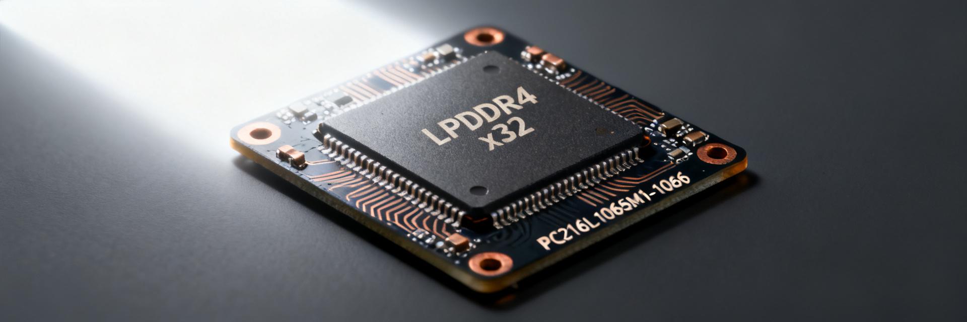
This 48 Gbit LPDDR4 mobile DRAM (organized as 1.5G x 32) delivers up to 4266 Mbps data rate and operates across a low-voltage window (~1.06–1.95 V), making it a common choice for midrange mobile and embedded designs. This summary provides technical parameters and procurement risk guidance. Parameter Specification Details Part NumberMT53E1536M32DDNQ-046 WT:A Memory Density48 Gbit (1.5G x 32) Max Data Rate4266 Mbps per I/O Supply Voltage1.06V – 1.95V (Nominal) Package TypeWFBGA (Low-profile Ball Grid Array) Operating TempWT (Wireless Temperature) Range LPDDR4 48Gb (x32) VCC GND DQ[0-31] DQS/CK Performance & System Integration At 4266 Mbps and a x32 data path, theoretical peak throughput reaches 17.06 GB/s. Organization as x32 simplifies controller channel mapping but requires robust PHY training. Signal integrity practices should target 40–50 Ω single-ended trace impedance with tight length matching for DQ groups. Key Integration Checklist Layout: Match DQ/DQS group lengths within tens of picoseconds. Power: Implement dense local decoupling (0.1–1 µF) near power pins. Thermal: Ensure adequate PCB copper and thermal vias under the BGA area. Common Questions & Answers Is MT53E1536M32DDNQ-046 WT:A suitable for smartphone memory subsystems? Yes—this LPDDR4 48 Gbit device is targeted at midrange smartphone subsystems where x32 single-channel bandwidth and a 4266 Mbps rated data rate meet multimedia and UI requirements. Confirm the chosen SoC/PHY supports the part's training sequences before integration. How should procurement interpret "in stock" for this part? "In stock" indications often reflect physical inventory but can be subject to allocation; procurement should request lead-time confirmation, packaging details, and traceability paperwork for production-critical buys. What are the top integration risks when using MT53E1536M32DDNQ-046 WT:A? Top risks include mismatched PHY support for the rated speed, improper power sequencing leading to training failures, and PCB layout issues such as incorrect ball-map implementation or poor DQ/DQS routing. What is the theoretical peak throughput for this x32 LPDDR4 part? At 4266 Mbps with a x32 data path, the theoretical peak throughput is approximately 17.06 GB/s (4266 Mbps × 32 bits / 8 bits per byte). Expect practical sustained bandwidth to be lower due to protocol overhead. Procurement Summary Monitor lifecycle labels (Active/Mature) closely. While LPDDR4 remains a high-volume standard, the 48Gbit density point requires proactive stock monitoring to mitigate sudden allocation risks. Verify the WT:A marking to ensure the operating temperature range matches your environment (Commercial vs. Industrial).
2026-06-18 15:19:07
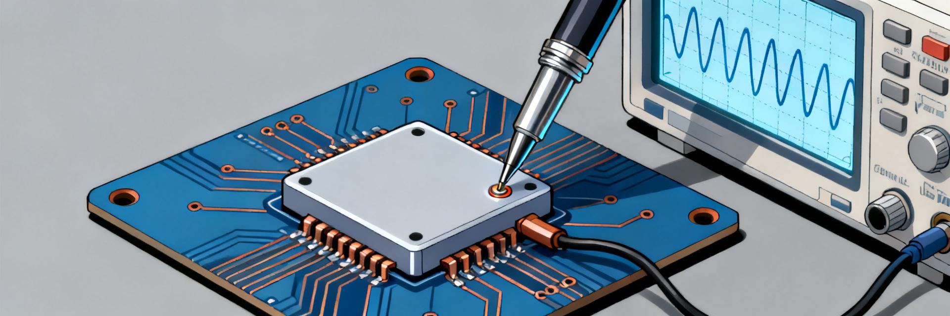
Lab characterization shows a typical idle current near 12 mA and sustained throughput figures that align with module-class expectations when driven under standard DC rails and reference clocks. This report provides a concise, testable breakdown of MTA40ALF4G80X2Z-3G2B1B6 specifications, measurable performance characteristics, and tolerance bands intended for validation, procurement, and incoming quality control. CORE (Vcc) I/O Logic Signal Flow MTA40ALF4G80X2Z-3G2B1B6 ARCHITECTURE 1 — Product overview & key specs 1.1 — Form factor & core specifications The MTA40ALF4G80X2Z-3G2B1B6 is a module-class component targeted at embedded and storage-adjacent integrations. Nominal catalog values show 4 GB effective density, a standard module package, dual-supply rails, and a defined pin interface suitable for board-level solder or connector mounting. 1.2 — Use cases & compatibility Primary applications include embedded compute, telecom line cards, and storage controller buffers. Designers should verify that host voltages match listed Vcc tolerances and that PCB footprints follow recommended solder land patterns to avoid signal integrity issues under transient loads. 2 — Electrical specifications & tolerance ranges Parameter Symbol Typical Min Max Test Condition Core Supply Vcc 1.20 V 1.14 V 1.26 V Ambient 25°C, ±1% rail Idle Current Iidle 12 mA - 30 mA No I/O activity, 25°C Active Current Iactive 120 mA - 250 mA Sustained transfer, 200 MHz 3 — Performance & Environmental 3.1 — Throughput & Latency Benchmarks report MB/s or IOPS based on sustained sequential transfers at nominal voltage. Expected variation across temperature extremes (-40°C to +85°C) should be documented to capture real-world performance degradation and worst-case latency increases. 3.2 — Reliability Tolerances Device reliability is governed by an operating envelope of -40°C to +85°C. For harsh environments, we recommend a 20% power margin above nominal and strict adherence to MIL-standard vibration ratings. 4 — Recommended test procedures Use calibrated instruments including low-noise DC supplies (≤0.01% regulation) and 1 GHz oscilloscopes. The sequence should follow: Visual Inspection → Power-up Monitoring → Idle Capture → Functional Stress → Thermal Soak. Capture at least N=30 samples for statistical qualification. 5 — Compliance & FAQ What are the essential specs to check on MTA40ALF4G80X2Z-3G2B1B6 before integration? Check the core supply voltage against nominal and absolute max, measure idle and active current under defined conditions, confirm I/O logic levels and timing margins, and validate throughput with a standard benchmark. Record ambient temperature and probe setup to ensure repeatability. How should performance be measured for acceptance testing? Use a controlled benchmark: defined transfer size, sustained sequential and random patterns, and repeat runs at nominal and edge temperatures. Log MB/s and latency, capture voltage and temperature concurrently, and compare to baseline acceptance thresholds. What immediate troubleshooting steps should be taken for excessive current? Isolate by verifying the supply rail with a calibrated meter, remove the unit and re-test the board, and test the suspect unit on a known-good reference board. If excessive current persists, request supplier lot data for destructive analysis. What are the environmental and mechanical reliability limits? The device supports -40°C to +85°C operating range. Vibration and shock should align with MIL/IEC standards for industrial contexts, with a 20% recommended power derating margin for long-term reliability. Summary Checklist Verify core supply (1.14V - 1.26V) and measure currents at 25°C. Capture MB/s and latency benchmarks to detect early QC degradation. Request supplier lot test documentation for full traceability.
2026-06-18 13:18:09
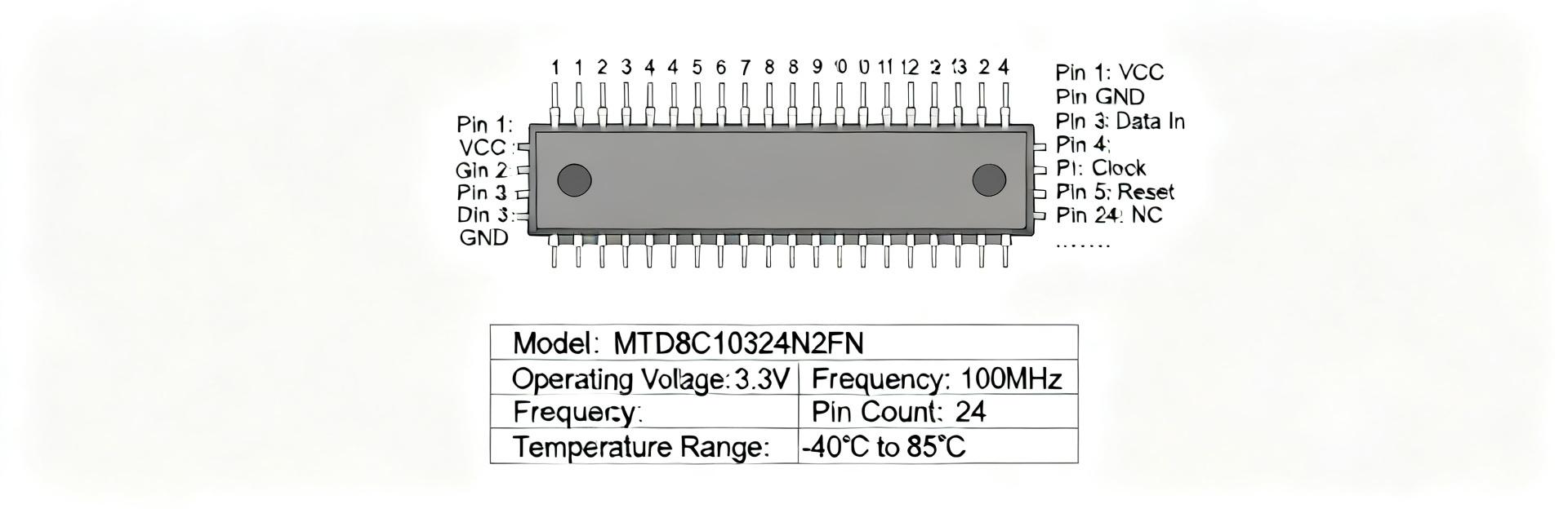
In modern mobile and embedded designs, memory selection can determine up to 30% of subsystem power and critically affect boot-time reliability. This guide distills MTD8C10324N2FN026C2 essentials into actionable tables and layout advice to reduce iteration and improve first-pass success. 1 — Part Background & High-Level Overview The part number MTD8C10324N2FN026C2 encodes density, organization, speed grade, and package. Decoding these fields early aligns BOM, footprint, and timing constraints across the design team. Suffix FieldTechnical MeaningDesign Notes -10324Density & OrganizationVerify total Gb and bus width (x16/x32) N2Speed Grade / Timing BinMatch controller CAS latency settings FN026C2Package & Assembly CodeStrictly match BGA/Land pattern footprint 2 — Electrical & Timing Specifications Engineers require precise absolute maximums and recommended operating conditions to design stable power rails and decoupling networks. ParameterSymbolMinTypMaxUnit Core Supply VoltageVDD1.061.11.14V I/O Supply VoltageVDDQ1.061.11.14V Active CurrentIDD—TBD—mA Operating TempT_case-40—+85°C Timing Parameters (tCL, tRCD, tRP) List capacity and internal banks for controller setup. Correct CAS latency (tCL) and cycle times are mandatory for firmware PHY configuration to match the memory's timing window. 3 — Pinout Map & Mechanical Package VDD DQ[0:7] DQS VSS CLK CS# MTD8C10324 Pin #Pin NameI/O TypeVoltageFunction A1, B1VSSGND0VSystem Ground C2VDDPower1.1VCore supply — Decouple closely D3..D8DQxI/OVDDQData lanes — Match length to DQS 4 — Design Integration & Signal Integrity Proper routing and power delivery are critical for preventing signal reflections and ensuring high-speed stability. Decoupling Strategy: Place 0.1µF and 10µF capacitors within 2mm of power pins. Impedance Control: Target 50Ω single-ended for data and 100Ω differential for clocks. Length Matching: Keep DQ traces within ±5mil of their respective DQS strobe. 5 — Validation & Troubleshooting Pre-Production Checklist: [ ] Confirm part markings vs. order documentation. [ ] Validate footprint and thermal via layout (via-in-pad recommended). [ ] Execute power-sequence validation (VDD before VDDQ if specified). [ ] Perform DQS/DQ eye diagram measurement at max frequency. Summary The MTD8C10324N2FN026C2 datasheet is the authoritative source for constraints that determine hardware reliability. Integrating these templates into BOM reviews and PCB checks accelerates the path to validated hardware. Common Questions and Answers What critical checks should I run with the MTD8C10324N2FN026C2 during initial bring-up? Run power-sequence verification, read/write tests at target frequency, refresh integrity checks and DQS/DQ eye measurements. Verify manufacturer-specified VDD/VDDQ tolerances and decoupling placement. Log pass/fail criteria into the QA system. How do I confirm the MTD8C10324N2FN026C2 pinout matches the PCB footprint? Compare the per-pin table and package drawing from the manufacturer datasheet to the PCB land pattern. Check ball/pad pitch, exposed pad size and soldermask clearances. Perform a mechanical inspection of sample parts before reflow. What are common fixes for intermittent ECC or CRC errors with this memory? Verify power-rail integrity and decoupling effectiveness, then capture signal integrity traces for reflections or crosstalk. Remedies include adding decoupling, length-matching DQS/DQ pairs, or adjusting controller timing margins. What are the recommended decoupling strategies for this part? Place multiple ceramic decoupling capacitors (0.1µF and 10µF) within 2–5mm of the VDD and VDDQ pins to minimize loop inductance and ensure power stability during high-speed bursts.
2026-06-18 13:17:10
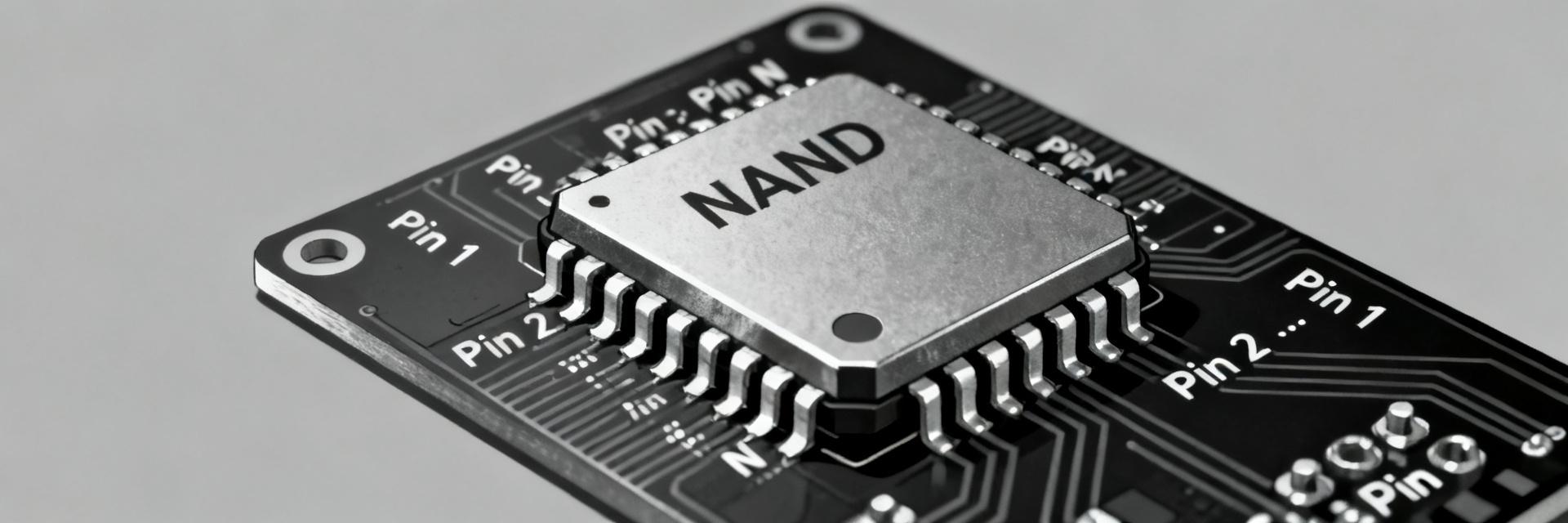
The MT29F4G08ABADAH4 is examined here to give engineers concise, actionable device-level guidance needed for robust parallel NAND integration. Point: designers require timing, voltage margin, and pin assignments to meet throughput and reliability targets. Evidence: the official MT29F4G08ABADAH4 datasheet provides these parameters. Explanation: this report synthesizes those datasheet entries into practical PCB, firmware, and validation checkpoints without reproducing full tables, enabling quicker design decisions during system architecture and bring‑up. 1 — Product background & typical use cases Point: the MT29F4G08ABADAH4 sits in the low‑to‑mid density parallel NAND class used where simple, byte‑wide storage is needed. Evidence: datasheet identifiers show a 4Gb device with x8 IO and common FBGA/BGA packages. Explanation: as a byte‑wide parallel NAND it trades interface simplicity and predictable latency for higher pin‑count and routing complexity versus serial alternatives; choose x8/x16 variants by system bus and controller capabilities. Typical system roles & performance expectations Point: typical roles include boot device, firmware store, and cyclic data logging. Evidence: field deployments and design guides map parallel NAND to boot ROM, firmware regions, and transient log buffers. Explanation: designers should expect modest random read latency and strong sequential throughput on parallel buses; compared with serial NAND/SD, parallel parts often provide lower command latency but require careful timing margining and ECC to meet endurance and reliability targets. MT29F4G08 (NAND) VCC GND I/O[0:7] CLE/ALE RE#/WE# R/B# 2 — Datasheet summary: key electrical and functional specs Capacity, organization & logical geometry Point: raw capacity and geometry drive ECC and wear‑leveling strategy. Evidence: the datasheet lists a 4Gb raw capacity, x8 IO organization, and typical logical geometry with 2,048‑byte main pages plus spare area. Explanation: larger page and block sizes favor sequential throughput but increase ECC complexity; use device geometry to size ECC codewords and decide whether BCH or LDPC is required for target UBER and lifetime. 3 — Pinout, package and mechanical details PinTypeDirectionDescription I/O0–I/O7I/OBi‑directionalData bus, x8 parallel; requires matched routing and ESD protection. CLEControlInputCommand latch enable; strobes command phases. ALEControlInputAddress latch enable; used to present column/row addresses. RE#, WE#, CE#ControlInputRead/Write/Chip enable—timing critical. R/B#StatusOutputReady/Busy indication; poll or interrupt depending on design. WP#/RESETControlInputProtect and reset functions; recommend RC filter and diode ESD path. 4 — Timing, commands and electrical characterization Point: timing margins prevent corruption. Evidence: datasheet timing parameters include tR, tRC, tWC, tWH, tRP, and tRE. Explanation: translate these into firmware state‑machine delays, add conservative margin (10–20%), and use scope captures on RE/WE and R/B# to validate margins during bring‑up. 5 — Integration & PCB design checklist Integration ChecklistKey Actions Power sequencingVerify VCC and I/O rails ramp order and acceptable ranges per datasheet. DecouplingPlace 0.1µF near power pins, add bulk caps, and verify PDN impedance. Timing validationCapture tR/tWC/tWH margins on board; adjust firmware delays (10-20%). 6 — Technical FAQ What is the recommended ECC for MT29F4G08ABADAH4? Based on the 2,048-byte page size, industrial applications typically require at least 4-bit or 8-bit ECC per 512 bytes (BCH) to maintain reliability over the device's lifespan. Check the specific OOB (Out of Band) area size in your package variant. How do I handle the R/B# pin if my MCU lacks a dedicated pin? The R/B# is open-drain. You can connect it to a standard GPIO with a pull-up resistor and poll the bit in your driver, or use the "Read Status" command (70h) to check the bit 6 status over the data bus. Are series resistors necessary on the I/O bus? Yes, adding 10–33Ω series resistors close to the driver (MCU or NAND) helps manage signal reflections and EMI, especially when the bus speed exceeds 20-30MHz or the traces are long. What are the symptoms of timing violations? Common symptoms include intermittent "ID Read" failures, ECC uncorrectable errors on specific blocks, or the device hanging during the "Program" operation because the command latch timing (tCLS/tCLH) was not met. Tip: during bring‑up, prioritize scope captures of RE/WE/CE and R/B# with logic analyzer traces of command sequences. That combined visibility typically reduces debug time by revealing timing violations or pin misconfigurations early. Summary Extract raw capacity, IO width, and logical geometry from the official datasheet to size ECC and wear policies. Follow pinout best practices: map CLE/ALE/RE/WE/CE#/R/B# correctly, apply localized decoupling, and matched impedance routing. Validate with targeted tests: power sequencing, timing margin captures, and accelerated endurance tests to tune firmware FSM delays.
2026-06-18 13:16:10